- 您现在的位置:买卖IC网 > Sheet目录2000 > IDT5T940-10NLGI (IDT, Integrated Device Technology Inc)IC CLK GENERATOR PREC 28-VFQFPN
2
INDUSTRIALTEMPERATURERANGE
IDT5T940
PRECISION CLOCKGENERATOROC-192 APPLICATIONS
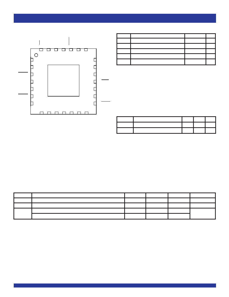
PIN CONFIGURATION
NOTE:
1. Stresses beyond those listed under ABSOLUTE MAXIMUM RATINGS may cause
permanent damage to the device. These are stress ratings only, and functional
operation of the device at these or any other conditions above those indicated in the
operational sections of this specification is not implied. Exposure to absolute-
maximum-rated conditions for extended periods may affect device reliability.
ABSOLUTE MAXIMUM RATINGS(1)
Symbol
Description
Max
Unit
VDD
Power Supply Voltage
–0.5 to +4.1
V
VI
Input Voltage
–0.5 to +4.1
V
VO
Output Voltage
–0.5 to VDD+0.5
V
TJ
Junction Temperature
150
°C
TSTG
Storage Temperature
–65 to +165
°C
NOTE:
1. Capacitance applies to all inputs except CLK/REF[1:0] and SELmode.
CAPACITANCE(TA=+25°C,f=1MHz,VIN=0V)
Parameter
Description
Typ.
Max.
Unit
CIN
InputCapacitance
2.5
3
pF
COUT
OutputCapacitance
—
pF
VFQFPN
TOP VIEW
GND
CLKIN
GND
REFIN
GND
VDD
GND
QREG
LOCK
GND
VDD
V
D
C
L
K
/R
E
F
1
C
L
K
/R
E
F
0
S
E
L
M
O
D
E
V
D
P
L
B
W
0
P
L
B
W
1
P
D
V
D
G
N
D
Q
O
U
T
Q
O
U
T
G
N
D
V
D
1
2
3
4
5
6
7
21
20
19
18
17
16
15
8
9
10
11
12
13
14
28
27
26
25
24
23
22
GND
Symbol
Description
Min.
Typ.
Max.
Unit
TA
AmbientOperatingTemperature
–40
+25
+85
°C
VDD
Power Supply Voltage
2.375
—
3.465
V
VT
TerminationVoltage(LVPECL)
—
VDD – 2
—
V
TerminationVoltage(LVDS)
—
1.2
—
RECOMMENDED OPERATING RANGE
发布紧急采购,3分钟左右您将得到回复。
相关PDF资料
IDT5T9820NLI8
IC CLK DRIVER ZD PLL 68-VFQFPN
IDT5T9890NLI8
IC CLK DRIVER 2.5V PLL 68-VFQFPN
IDT5V19EE604NDGI8
IC PLL CLK GEN 200MHZ 28VFQFPN
IDT5V40501DVG
IC CLK GEN PLL 160MHZ 8TSSOP
IDT5V41064NLGI
IC CLK GEN 1:1 16QFN
IDT5V41066PGG
IC CLK GEN SPRED SPECTRM 20TSSOP
IDT5V49EE901NLGI8
IC PLL CLK GEN 200MHZ 32VFQFN
IDT5V49EE902NLGI
IC CLOCK GEN PLL 500MHZ 32VFQFPN
相关代理商/技术参数
IDT5T940-10NLGI8
功能描述:IC CLK GENERATOR PREC 28-VFQFPN RoHS:是 类别:集成电路 (IC) >> 时钟/计时 - 专用 系列:- 标准包装:1,500 系列:- 类型:时钟缓冲器/驱动器 PLL:是 主要目的:- 输入:- 输出:- 电路数:- 比率 - 输入:输出:- 差分 - 输入:输出:- 频率 - 最大:- 电源电压:3.3V 工作温度:0°C ~ 70°C 安装类型:表面贴装 封装/外壳:28-SSOP(0.209",5.30mm 宽) 供应商设备封装:28-SSOP 包装:带卷 (TR) 其它名称:93786AFT
IDT5T940-30NLGI
功能描述:IC CLK GENERATOR PREC 28-VFQFPN RoHS:是 类别:集成电路 (IC) >> 时钟/计时 - 专用 系列:- 标准包装:1 系列:- 类型:时钟/频率发生器,多路复用器 PLL:是 主要目的:存储器,RDRAM 输入:晶体 输出:LVCMOS 电路数:1 比率 - 输入:输出:1:2 差分 - 输入:输出:无/是 频率 - 最大:400MHz 电源电压:3 V ~ 3.6 V 工作温度:0°C ~ 85°C 安装类型:表面贴装 封装/外壳:16-TSSOP(0.173",4.40mm 宽) 供应商设备封装:16-TSSOP 包装:Digi-Reel® 其它名称:296-6719-6
IDT5T940-30NLGI8
功能描述:IC CLK GENERATOR PREC 28-VFQFPN RoHS:是 类别:集成电路 (IC) >> 时钟/计时 - 专用 系列:- 标准包装:1,500 系列:- 类型:时钟缓冲器/驱动器 PLL:是 主要目的:- 输入:- 输出:- 电路数:- 比率 - 输入:输出:- 差分 - 输入:输出:- 频率 - 最大:- 电源电压:3.3V 工作温度:0°C ~ 70°C 安装类型:表面贴装 封装/外壳:28-SSOP(0.209",5.30mm 宽) 供应商设备封装:28-SSOP 包装:带卷 (TR) 其它名称:93786AFT
IDT5T9820NLGI
功能描述:IC CLK DRIVER ZD PLL 68-VFQFPN RoHS:是 类别:集成电路 (IC) >> 时钟/计时 - 时钟发生器,PLL,频率合成器 系列:- 标准包装:39 系列:- 类型:* PLL:带旁路 输入:时钟 输出:时钟 电路数:1 比率 - 输入:输出:1:10 差分 - 输入:输出:是/是 频率 - 最大:170MHz 除法器/乘法器:无/无 电源电压:2.375 V ~ 3.465 V 工作温度:0°C ~ 70°C 安装类型:* 封装/外壳:* 供应商设备封装:* 包装:*
IDT5T9820NLGI8
功能描述:IC CLK DRIVER ZD PLL 68-VFQFPN RoHS:是 类别:集成电路 (IC) >> 时钟/计时 - 时钟发生器,PLL,频率合成器 系列:- 标准包装:39 系列:- 类型:* PLL:带旁路 输入:时钟 输出:时钟 电路数:1 比率 - 输入:输出:1:10 差分 - 输入:输出:是/是 频率 - 最大:170MHz 除法器/乘法器:无/无 电源电压:2.375 V ~ 3.465 V 工作温度:0°C ~ 70°C 安装类型:* 封装/外壳:* 供应商设备封装:* 包装:*
IDT5T9820NLI
功能描述:IC CLK DRIVER ZD PLL 68-VFQFPN RoHS:否 类别:集成电路 (IC) >> 时钟/计时 - 时钟发生器,PLL,频率合成器 系列:- 标准包装:39 系列:- 类型:* PLL:带旁路 输入:时钟 输出:时钟 电路数:1 比率 - 输入:输出:1:10 差分 - 输入:输出:是/是 频率 - 最大:170MHz 除法器/乘法器:无/无 电源电压:2.375 V ~ 3.465 V 工作温度:0°C ~ 70°C 安装类型:* 封装/外壳:* 供应商设备封装:* 包装:*
IDT5T9820NLI8
功能描述:IC CLK DRIVER ZD PLL 68-VFQFPN RoHS:否 类别:集成电路 (IC) >> 时钟/计时 - 时钟发生器,PLL,频率合成器 系列:- 标准包装:39 系列:- 类型:* PLL:带旁路 输入:时钟 输出:时钟 电路数:1 比率 - 输入:输出:1:10 差分 - 输入:输出:是/是 频率 - 最大:170MHz 除法器/乘法器:无/无 电源电压:2.375 V ~ 3.465 V 工作温度:0°C ~ 70°C 安装类型:* 封装/外壳:* 供应商设备封装:* 包装:*
IDT5T9821NLGI
功能描述:IC CLK DRIVER ZD PLL 68-VFQFPN RoHS:是 类别:集成电路 (IC) >> 时钟/计时 - 时钟发生器,PLL,频率合成器 系列:- 标准包装:39 系列:- 类型:* PLL:带旁路 输入:时钟 输出:时钟 电路数:1 比率 - 输入:输出:1:10 差分 - 输入:输出:是/是 频率 - 最大:170MHz 除法器/乘法器:无/无 电源电压:2.375 V ~ 3.465 V 工作温度:0°C ~ 70°C 安装类型:* 封装/外壳:* 供应商设备封装:* 包装:*